- 您现在的位置:买卖IC网 > Sheet目录2007 > LTC7545ACG#TRPBF (Linear Technology)IC D/ACONV MULTIPLY 12BIT 20SSOP
3
LTC7545A
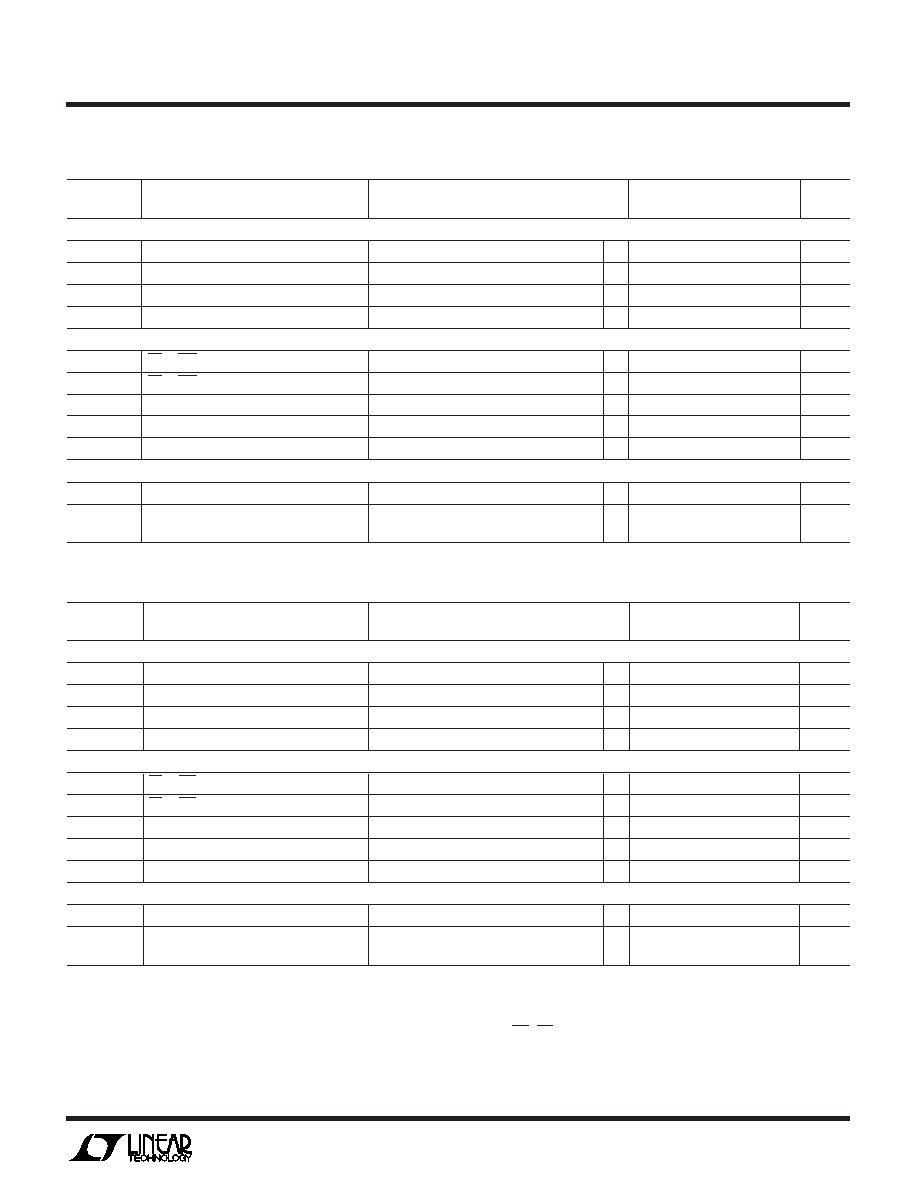
ELECTRICAL CHARACTERISTICS
VDD = 5V, VREF = 10V, VOUT1 = AGND = 0V, TA = TMIN to TMAX, unless otherwise noted.
ALL GRADES
SYMBOL
PARAMETER
CONDITIONS
MIN
TYP
MAX
UNITS
Digital Inputs
VIH
Digital Input High Voltage
q
2.4
V
VIL
Digital Input Low Voltage
q
0.8
V
IIN
Digital Input Current
q
0.001
±1
A
CIN
Digital Input Capacitance
(Note 3) VIN = 0V
q
8pF
Timing Characteristics (Note 3)
tCS
CS to WR Setup Time
q
100
ns
tCH
CS to WR Hold Time
q
0ns
tWR
Write Pulse Width
q
100
ns
tDS
Data Setup Time
q
100
ns
tDH
Data Hold Time
q
5ns
Power Supply
VDD
Supply Voltage
q
4.75
5
5.25
V
IDD
Supply Current
All Digital Inputs = VIH or VIL
q
2mA
All Digital Inputs = 0V or VDD
q
10
100
A
VDD = 15V, VREF = 10V, VOUT1 = AGND = 0V, TA = TMIN to TMAX, unless otherwise noted.
The q denotes specificatons which apply over the full operating
temperature range.
Note 1:
±0.5LSB = ±0.012% of full scale.
Note 2: Using internal feedback resistor.
Note 3: Guaranteed by design, not subject to test.
Note 4: IOUT1 with DAC register loaded to all 0s.
Note 5: Typical temperature coefficient is 100ppm/
°C.
Note 6: OUT1 load = 100
in parallel with 13pF.
Note 7: To 0.01% for a full-scale change, measured from the falling
edge of WR, CS = 0V.
Note 8: From digital input change to 90% of final analog output.
Note 9: VREF = 0V. DAC register contents changed from all 0s to all 1s
or all 1s to all 0s.
ALL GRADES
SYMBOL
PARAMETER
CONDITIONS
MIN
TYP
MAX
UNITS
Digital Inputs
VIH
Digital Input High Voltage
q
13.5
V
VIL
Digital Input Low Voltage
q
1.5
V
IIN
Digital Input Current
q
±1
A
CIN
Digital Input Capacitance
(Note 3) VIN = 0V
q
8pF
Timing Characteristics (Note 3)
tCS
CS to WR Setup Time
q
75
ns
tCH
CS to WR Hold Time
q
0ns
tWR
Write Pulse Width
q
75
ns
tDS
Data Setup Time
q
60
ns
tDH
Data Hold Time
q
5ns
Power Supply
VDD
Supply Voltage
q
14.25
15
15.75
V
IDD
Supply Current
All Digital Inputs = VIH or VIL
q
2mA
All Digital Inputs = 0V or VDD
q
10
100
A
发布紧急采购,3分钟左右您将得到回复。
相关PDF资料
LTC8043EN8
IC D/A CONV 12BIT SERIAL 8-DIP
LTC8143ESW#TRPBF
IC D/A CONV 12BIT SERIAL 16-SOIC
LTM9011CY-14#PBF
IC ADC 14BIT UMODULE 140BGA
LV5609LP-E
IC CLOCK DRIVER VERTICAL 24VCT
LV5609LP-TE-L-E
IC CLOCK DRIVER VERT VCT24
M-986-2A1PL
IC TRANSCEIVER MF 2CHAN 44-PLCC
MAX038CWP+
IC GEN WAVEFORM HI-FREQ 20-SOIC
MAX1002CAX+T
IC ADC 6BIT 60MSPS DUAL 36-SSOP
相关代理商/技术参数
LTC7545ACN
功能描述:IC D/A CONV 12BIT PARALLEL 20DIP RoHS:否 类别:集成电路 (IC) >> 数据采集 - 数模转换器 系列:- 产品培训模块:LTC263x 12-, 10-, and 8-Bit VOUT DAC Family 特色产品:LTC2636 - Octal 12-/10-/8-Bit SPI VOUT DACs with 10ppm/°C Reference 标准包装:91 系列:- 设置时间:4µs 位数:10 数据接口:MICROWIRE?,串行,SPI? 转换器数目:8 电压电源:单电源 功率耗散(最大):2.7mW 工作温度:-40°C ~ 85°C 安装类型:表面贴装 封装/外壳:14-WFDFN 裸露焊盘 供应商设备封装:14-DFN-EP(4x3) 包装:管件 输出数目和类型:8 电压,单极 采样率(每秒):*
LTC7545ACN#PBF
功能描述:IC D/A CONV 12BIT PARALLEL 20DIP RoHS:是 类别:集成电路 (IC) >> 数据采集 - 数模转换器 系列:- 产品培训模块:LTC263x 12-, 10-, and 8-Bit VOUT DAC Family 特色产品:LTC2636 - Octal 12-/10-/8-Bit SPI VOUT DACs with 10ppm/°C Reference 标准包装:91 系列:- 设置时间:4µs 位数:10 数据接口:MICROWIRE?,串行,SPI? 转换器数目:8 电压电源:单电源 功率耗散(最大):2.7mW 工作温度:-40°C ~ 85°C 安装类型:表面贴装 封装/外壳:14-WFDFN 裸露焊盘 供应商设备封装:14-DFN-EP(4x3) 包装:管件 输出数目和类型:8 电压,单极 采样率(每秒):*
LTC7545ACSW
功能描述:IC D/A CONV 12BIT PARALLEL20SOIC RoHS:否 类别:集成电路 (IC) >> 数据采集 - 数模转换器 系列:- 产品培训模块:LTC263x 12-, 10-, and 8-Bit VOUT DAC Family 特色产品:LTC2636 - Octal 12-/10-/8-Bit SPI VOUT DACs with 10ppm/°C Reference 标准包装:91 系列:- 设置时间:4µs 位数:10 数据接口:MICROWIRE?,串行,SPI? 转换器数目:8 电压电源:单电源 功率耗散(最大):2.7mW 工作温度:-40°C ~ 85°C 安装类型:表面贴装 封装/外壳:14-WFDFN 裸露焊盘 供应商设备封装:14-DFN-EP(4x3) 包装:管件 输出数目和类型:8 电压,单极 采样率(每秒):*
LTC7545ACSW#PBF
功能描述:IC D/A CONV 12BIT PARALLEL20SOIC RoHS:是 类别:集成电路 (IC) >> 数据采集 - 数模转换器 系列:- 产品培训模块:LTC263x 12-, 10-, and 8-Bit VOUT DAC Family 特色产品:LTC2636 - Octal 12-/10-/8-Bit SPI VOUT DACs with 10ppm/°C Reference 标准包装:91 系列:- 设置时间:4µs 位数:10 数据接口:MICROWIRE?,串行,SPI? 转换器数目:8 电压电源:单电源 功率耗散(最大):2.7mW 工作温度:-40°C ~ 85°C 安装类型:表面贴装 封装/外壳:14-WFDFN 裸露焊盘 供应商设备封装:14-DFN-EP(4x3) 包装:管件 输出数目和类型:8 电压,单极 采样率(每秒):*
LTC7545ACSW#TR
功能描述:IC DAC 12BIT PAR MULTIPLY 20SOIC RoHS:否 类别:集成电路 (IC) >> 数据采集 - 数模转换器 系列:- 产品培训模块:LTC263x 12-, 10-, and 8-Bit VOUT DAC Family 特色产品:LTC2636 - Octal 12-/10-/8-Bit SPI VOUT DACs with 10ppm/°C Reference 标准包装:91 系列:- 设置时间:4µs 位数:10 数据接口:MICROWIRE?,串行,SPI? 转换器数目:8 电压电源:单电源 功率耗散(最大):2.7mW 工作温度:-40°C ~ 85°C 安装类型:表面贴装 封装/外壳:14-WFDFN 裸露焊盘 供应商设备封装:14-DFN-EP(4x3) 包装:管件 输出数目和类型:8 电压,单极 采样率(每秒):*
LTC7545ACSW#TRPBF
功能描述:IC D/A CONV 12BIT PARALLEL20SOIC RoHS:是 类别:集成电路 (IC) >> 数据采集 - 数模转换器 系列:- 产品培训模块:LTC263x 12-, 10-, and 8-Bit VOUT DAC Family 特色产品:LTC2636 - Octal 12-/10-/8-Bit SPI VOUT DACs with 10ppm/°C Reference 标准包装:91 系列:- 设置时间:4µs 位数:10 数据接口:MICROWIRE?,串行,SPI? 转换器数目:8 电压电源:单电源 功率耗散(最大):2.7mW 工作温度:-40°C ~ 85°C 安装类型:表面贴装 封装/外壳:14-WFDFN 裸露焊盘 供应商设备封装:14-DFN-EP(4x3) 包装:管件 输出数目和类型:8 电压,单极 采样率(每秒):*
LTC7545AKG
功能描述:IC D/ACONV MULTIPLY 12BIT 20SSOP RoHS:否 类别:集成电路 (IC) >> 数据采集 - 数模转换器 系列:- 产品培训模块:LTC263x 12-, 10-, and 8-Bit VOUT DAC Family 特色产品:LTC2636 - Octal 12-/10-/8-Bit SPI VOUT DACs with 10ppm/°C Reference 标准包装:91 系列:- 设置时间:4µs 位数:10 数据接口:MICROWIRE?,串行,SPI? 转换器数目:8 电压电源:单电源 功率耗散(最大):2.7mW 工作温度:-40°C ~ 85°C 安装类型:表面贴装 封装/外壳:14-WFDFN 裸露焊盘 供应商设备封装:14-DFN-EP(4x3) 包装:管件 输出数目和类型:8 电压,单极 采样率(每秒):*
LTC7545AKG#PBF
功能描述:IC D/ACONV MULTIPLY 12BIT 20SSOP RoHS:是 类别:集成电路 (IC) >> 数据采集 - 数模转换器 系列:- 产品培训模块:LTC263x 12-, 10-, and 8-Bit VOUT DAC Family 特色产品:LTC2636 - Octal 12-/10-/8-Bit SPI VOUT DACs with 10ppm/°C Reference 标准包装:91 系列:- 设置时间:4µs 位数:10 数据接口:MICROWIRE?,串行,SPI? 转换器数目:8 电压电源:单电源 功率耗散(最大):2.7mW 工作温度:-40°C ~ 85°C 安装类型:表面贴装 封装/外壳:14-WFDFN 裸露焊盘 供应商设备封装:14-DFN-EP(4x3) 包装:管件 输出数目和类型:8 电压,单极 采样率(每秒):*